PCB Design
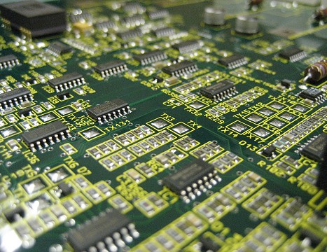
PCB design (Printed Circuit Board) can start as soon as the electronic circuit is fully known and also the desired shape of the circuit board (PCB). Of course, many factors play a role here, such as operating conditions, temperature range, enclosure dimensions, type of enclosure, EMC properties and availability of the chosen components.
What many people do not know is that the circuit board is also a component in the electrical circuit. As a result, the circuit board also determines EMC properties and electrical properties. The thickness and width of a track determines the amount of current that can be fed. The width and thickness of the insulation layers also determine the high-frequency behaviour of a connection. As a result, a change in the circuit board often means that the EMC properties have to be measured again!
Brunelco offers you the possibility to develop single-sided, double-sided or even multilayer PCBs up to 20 layers. This of course depends on the complexity of your desired control system. Components can be placed on one or both sides.

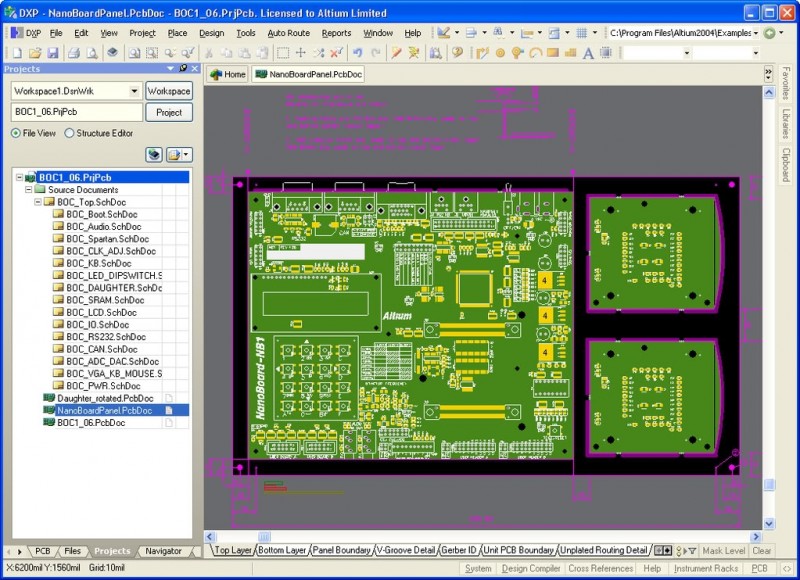
Our CAE/CAD systems offer our engineers all the possibilities; printed-circuit boards ranging from double-sided PCBs to complex multilayer, flex-rigid printing. We use the Altium Designer development environment.
Brunelco designs with both conventional plug-in and surface-mount technology with single-sided or double-sided mounting. This depends on the complexity of your circuit.


